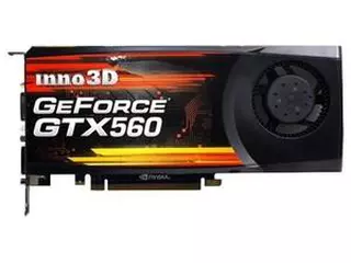
GeForce GTX 560 SE vs Radeon R8 M535DX
When comparing GeForce GTX 560 SE and Radeon R8 M535DX, we look primarily at benchmarks and game tests. But it is not only about the numbers. Often you can find third-party models with higher clock speeds, better cooling, or a customizable RGB lighting. Not all of them will have all the features you need. Another thing to consider is the port selection. Most graphics cards have at least one DisplayPort and HDMI interface, but some monitors require DVI. Before you buy, check the TDP of the graphics card - this characteristic will help you estimate the consumption of the graphics card. You may even have to upgrade your PSU to meet its requirements. An important factor when choosing between GeForce GTX 560 SE and Radeon R8 M535DX is the price. Does the additional cost justify the performance hit? Our comparison should help you make the right decision.
Radeon R8 M535DX
Main Specs
GeForce GTX 560 SE
Radeon R8 M535DX
Power consumption (TDP)
150 Watt
Interface
PCIe 2.0 x16
IGP
Supplementary power connectors
2x 6-pin
Memory type
GDDR5
System Shared
Maximum RAM amount
1 GB
Display Connectors
2x DVI, 1x mini-HDMI
No outputs
Check Price
GeForce GTX 560 SE is connected by PCIe 2.0 x16, and Radeon R8 M535DX uses IGP interface.
Both cards are used in Desktops.
GeForce GTX 560 SE is build with Fermi 2.0 architecture, and Radeon R8 M535DX - with GCN 3.0.
Core clock speed of Radeon R8 M535DX is 44 MHz higher, than GeForce GTX 560 SE.
GeForce GTX 560 SE is manufactured by 40 nm process technology, and Radeon R8 M535DX - by 28 nm process technology.
Game benchmarks
Assassin's Creed Odyssey
Battlefield 5
Call of Duty: Warzone
Counter-Strike: Global Offensive
Cyberpunk 2077
Dota 2
Far Cry 5
Fortnite
Forza Horizon 4
Grand Theft Auto V
Metro Exodus
Minecraft
PLAYERUNKNOWN'S BATTLEGROUNDS
Red Dead Redemption 2
The Witcher 3: Wild Hunt
World of Tanks
high / 1080p
9−10
0−1
ultra / 1080p
5−6
−
QHD / 1440p
0−1
0−1
low / 720p
21−24
1−2
medium / 1080p
10−12
0−1
The average gaming FPS of GeForce GTX 560 SE in Assassin's Creed Odyssey is 2100% more, than Radeon R8 M535DX.
high / 1080p
14−16
−
ultra / 1080p
12−14
−
QHD / 1440p
0−1
0−1
low / 720p
30−35
0−1
medium / 1080p
16−18
−
low / 768p
45−50
50−55
high / 1080p
−
45−50
QHD / 1440p
0−1
0−1
The average gaming FPS of Radeon R8 M535DX in Call of Duty: Warzone is 10% more, than GeForce GTX 560 SE.
low / 768p
160−170
60−65
medium / 768p
130−140
27−30
ultra / 1080p
65−70
7−8
QHD / 1440p
35−40
−
4K / 2160p
27−30
−
high / 768p
100−105
16−18
The average gaming FPS of GeForce GTX 560 SE in Counter-Strike: Global Offensive is 317% more, than Radeon R8 M535DX.
low / 768p
55−60
70−75
ultra / 1080p
24−27
0−1
medium / 1080p
45−50
45−50
The average gaming FPS of Radeon R8 M535DX in Cyberpunk 2077 is 15% more, than GeForce GTX 560 SE.
low / 768p
90−95
45−50
medium / 768p
70−75
10−11
ultra / 1080p
40−45
0−1
The average gaming FPS of GeForce GTX 560 SE in Dota 2 is 182% more, than Radeon R8 M535DX.
high / 1080p
10−12
−
ultra / 1080p
10−11
−
4K / 2160p
4−5
−
low / 720p
24−27
0−1
medium / 1080p
10−12
−
high / 1080p
16−18
−
ultra / 1080p
12−14
−
low / 720p
70−75
21−24
medium / 1080p
30−35
0−1
The average gaming FPS of GeForce GTX 560 SE in Fortnite is 227% more, than Radeon R8 M535DX.
high / 1080p
16−18
0−1
ultra / 1080p
12−14
−
QHD / 1440p
3−4
0−1
low / 720p
30−35
0−1
medium / 1080p
18−20
0−1
low / 768p
60−65
18−20
medium / 768p
55−60
−
high / 1080p
16−18
0−1
ultra / 1080p
8−9
−
QHD / 1440p
0−1
0−1
medium / 720p
−
12−14
The average gaming FPS of GeForce GTX 560 SE in Grand Theft Auto V is 226% more, than Radeon R8 M535DX.
high / 1080p
6−7
−
ultra / 1080p
4−5
−
4K / 2160p
1−2
−
low / 720p
16−18
0−1
medium / 1080p
8−9
−
low / 768p
100−105
75−80
high / 1080p
95−100
27−30
ultra / 1080p
85−90
−
medium / 1080p
95−100
−
The average gaming FPS of GeForce GTX 560 SE in Minecraft is 88% more, than Radeon R8 M535DX.
high / 1080p
18−20
−
ultra / 1080p
14−16
−
low / 720p
40−45
8−9
medium / 1080p
18−20
−
The average gaming FPS of GeForce GTX 560 SE in PLAYERUNKNOWN'S BATTLEGROUNDS is 425% more, than Radeon R8 M535DX.
high / 1080p
12−14
−
ultra / 1080p
8−9
−
QHD / 1440p
0−1
−
low / 720p
16−18
0−1
medium / 1080p
12−14
−
low / 768p
30−35
0−1
medium / 768p
21−24
−
high / 1080p
12−14
−
ultra / 1080p
7−8
−
4K / 2160p
6−7
−
low / 768p
90−95
45−50
medium / 768p
50−55
14−16
ultra / 1080p
24−27
0−1
high / 768p
40−45
12−14
The average gaming FPS of GeForce GTX 560 SE in World of Tanks is 148% more, than Radeon R8 M535DX.
Full Specs
GeForce GTX 560 SE
Radeon R8 M535DX
Architecture
Fermi 2.0
GCN 3.0
Code name
GF114
Meso
Type
Desktop
Desktop
Release date
20 February 2012
18 April 2017
Pipelines
288
320
Core clock speed
736 MHz
780 MHz
Boost Clock
891 MHz
Transistor count
1,950 million
1,550 million
Manufacturing process technology
40 nm
28 nm
Texture fill rate
35.33
17.82
Floating-point performance
847.9 gflops
Length
210 mm
Memory bus width
192 Bit
Memory clock speed
3828 MHz
Memory bandwidth
91.87 GB/s
DirectX
12 (11_0)
12 (12_0)
Shader Model
5.1
6.0
OpenGL
4.6
4.6
OpenCL
1.1
2.0
Vulkan
N/A
1.2.131
CUDA
2.1
Bitcoin / BTC (SHA256)
54 Mh/s
Check Price


