GeForce GTX 570 vs NVS 510
If you are going to buy a new graphics card and are choosing between GeForce GTX 570 and NVS 510, there are a couple of things to consider. Cards with more VRAM in general perform better and allow you to play on higher graphics settings. Size also makes a difference. A model with a large heatsink can occupy up to three expansion slots on a motherboard. Be sure you have enough room in your PC case. When comparing GPUs with different architectures, more processing cores and even higher TFLOPS will not always translate to better performance. To help you decide which GPU you need, we have measured frame rates in a number of popular games. For more on how the GeForce GTX 570 stacks up against NVS 510, check out specs charts below.
Main Specs
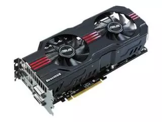
GeForce GTX 570
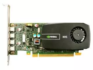
NVS 510
Power consumption (TDP)
219 Watt
35 Watt
Interface
PCIe 2.0 x16
PCIe 2.0 x16
Supplementary power connectors
Two 6-pin
None
Memory type
GDDR5
DDR3
Maximum RAM amount
1280 MB
2 GB
Display Connectors
2x DVI, 1x mini-HDMI
4x mini-DisplayPort
Check Price
Check Price
GeForce GTX 570 has 525% more power consumption, than NVS 510.
Both video cards are using PCIe 2.0 x16 interface connection to a motherboard.
GeForce GTX 570 has 1278 GB more memory, than NVS 510.
Both cards are used in Desktops.
GeForce GTX 570 is build with Fermi architecture, and NVS 510 - with Kepler.
Core clock speed of GeForce GTX 570 is 667 MHz higher, than NVS 510.
GeForce GTX 570 is manufactured by 40 nm process technology, and NVS 510 - by 28 nm process technology.
NVS 510 is 150 mm longer, than GeForce GTX 570.
Memory clock speed of GeForce GTX 570 is 118 MHz higher, than NVS 510.
Game benchmarks
Assassin's Creed Odyssey
Battlefield 5
Call of Duty: Warzone
Counter-Strike: Global Offensive
Cyberpunk 2077
Dota 2
Far Cry 5
Fortnite
Forza Horizon 4
Grand Theft Auto V
Metro Exodus
Minecraft
PLAYERUNKNOWN'S BATTLEGROUNDS
Red Dead Redemption 2
The Witcher 3: Wild Hunt
World of Tanks
high / 1080p
20−22
0−1
ultra / 1080p
12−14
−
QHD / 1440p
6−7
0−1
4K / 2160p
5−6
−
low / 720p
35−40
1−2
medium / 1080p
24−27
0−1
The average gaming FPS of GeForce GTX 570 in Assassin's Creed Odyssey is 3600% more, than NVS 510.
high / 1080p
30−35
−
ultra / 1080p
27−30
−
QHD / 1440p
10−12
0−1
4K / 2160p
7−8
−
low / 720p
65−70
0−1
medium / 1080p
35−40
−
low / 768p
50−55
50−55
high / 1080p
−
45−50
QHD / 1440p
0−1
0−1
GeForce GTX 570 and NVS 510 have the same average FPS in Call of Duty: Warzone.
low / 768p
230−240
60−65
medium / 768p
200−210
27−30
ultra / 1080p
110−120
7−8
QHD / 1440p
85−90
−
4K / 2160p
45−50
−
high / 768p
160−170
16−18
The average gaming FPS of GeForce GTX 570 in Counter-Strike: Global Offensive is 542% more, than NVS 510.
low / 768p
60−65
70−75
ultra / 1080p
50−55
0−1
medium / 1080p
55−60
45−50
GeForce GTX 570 and NVS 510 have the same average FPS in Cyberpunk 2077.
low / 768p
120−130
45−50
medium / 768p
100−110
10−11
ultra / 1080p
75−80
0−1
The average gaming FPS of GeForce GTX 570 in Dota 2 is 296% more, than NVS 510.
high / 1080p
24−27
−
ultra / 1080p
21−24
−
QHD / 1440p
18−20
−
4K / 2160p
7−8
−
low / 720p
50−55
0−1
medium / 1080p
24−27
−
high / 1080p
30−35
−
ultra / 1080p
24−27
−
QHD / 1440p
14−16
−
low / 720p
120−130
21−24
medium / 1080p
70−75
0−1
The average gaming FPS of GeForce GTX 570 in Fortnite is 468% more, than NVS 510.
high / 1080p
30−35
0−1
ultra / 1080p
24−27
−
QHD / 1440p
12−14
0−1
4K / 2160p
12−14
−
low / 720p
65−70
0−1
medium / 1080p
35−40
0−1
low / 768p
100−110
18−20
medium / 768p
90−95
−
high / 1080p
40−45
0−1
ultra / 1080p
16−18
−
QHD / 1440p
6−7
0−1
medium / 720p
−
12−14
The average gaming FPS of GeForce GTX 570 in Grand Theft Auto V is 452% more, than NVS 510.
high / 1080p
12−14
−
ultra / 1080p
10−11
−
4K / 2160p
2−3
−
low / 720p
35−40
0−1
medium / 1080p
16−18
−
low / 768p
120−130
75−80
high / 1080p
−
27−30
medium / 1080p
110−120
−
The average gaming FPS of GeForce GTX 570 in Minecraft is 62% more, than NVS 510.
ultra / 1080p
14−16
−
low / 720p
70−75
8−9
medium / 1080p
18−20
−
The average gaming FPS of GeForce GTX 570 in PLAYERUNKNOWN'S BATTLEGROUNDS is 800% more, than NVS 510.
high / 1080p
14−16
−
ultra / 1080p
10−11
−
QHD / 1440p
1−2
−
4K / 2160p
1−2
−
low / 720p
35−40
0−1
medium / 1080p
20−22
−
low / 768p
70−75
0−1
medium / 768p
45−50
−
high / 1080p
24−27
−
ultra / 1080p
14−16
−
4K / 2160p
8−9
−
low / 768p
90−95
45−50
medium / 768p
60−65
14−16
ultra / 1080p
40−45
0−1
high / 768p
55−60
12−14
The average gaming FPS of GeForce GTX 570 in World of Tanks is 180% more, than NVS 510.
Full Specs
GeForce GTX 570
NVS 510
Architecture
Fermi
Kepler
Code name
GF110
GK107
Type
Desktop
Workstation
Release date
7 December 2010
23 October 2012
Pipelines
480
192
Core clock speed
1464 MHz
797 MHz
Transistor count
3,000 million
1,270 million
Manufacturing process technology
40 nm
28 nm
Texture fill rate
43.9 billion/sec
12.75
Floating-point performance
1,405.4 gflops
306.0 gflops
Length
10.5" (267 mm) (26.7 cm)
160 mm
Memory bus width
320 Bit
128 Bit
Memory clock speed
1900 MHz (3800 data rate)
1782 MHz
Memory bandwidth
152.0 GB/s
28.51 GB/s
DirectX
12 (11_0)
12 (11_0)
Shader Model
5.1
5.1
OpenGL
4.2
4.6
OpenCL
1.1
1.2
Vulkan
N/A
1.1.126
CUDA
+
3.0
CUDA cores
480
Bus support
PCI-E 2.0 x 16
Height
4.376" (111 mm) (11.1 cm)
SLI options
+
Multi monitor support
+
HDMI
+
Maximum VGA resolution
2048x1536
Audio input for HDMI
Internal
Bitcoin / BTC (SHA256)
133 Mh/s
17 Mh/s
Ethereum / ETH (DaggerHashimoto)
13 Mh/s
Check Price
Check Price