GeForce 820A vs GeForce GTX 670
When comparing GeForce 820A and GeForce GTX 670, we look primarily at benchmarks and game tests. But it is not only about the numbers. Often you can find third-party models with higher clock speeds, better cooling, or a customizable RGB lighting. Not all of them will have all the features you need. Another thing to consider is the port selection. Most graphics cards have at least one DisplayPort and HDMI interface, but some monitors require DVI. Before you buy, check the TDP of the graphics card - this characteristic will help you estimate the consumption of the graphics card. You may even have to upgrade your PSU to meet its requirements. An important factor when choosing between GeForce 820A and GeForce GTX 670 is the price. Does the additional cost justify the performance hit? Our comparison should help you make the right decision.
GeForce 820A
Main Specs
GeForce 820A
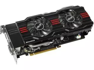
GeForce GTX 670
Power consumption (TDP)
15 Watt
170 Watt
Interface
PCIe 2.0 x16
PCIe 3.0 x16
Supplementary power connectors
Two 6-pin
Memory type
DDR3
GDDR5
Maximum RAM amount
1 GB
2 GB
Display Connectors
No outputs
2x DVI, 1x HDMI, 1x DisplayPort
Check Price
GeForce GTX 670 has 1033% more power consumption, than GeForce 820A.
GeForce 820A is connected by PCIe 2.0 x16, and GeForce GTX 670 uses PCIe 3.0 x16 interface.
GeForce GTX 670 has 1 GB more memory, than GeForce 820A.
Both cards are used in Desktops.
GeForce 820A is build with Fermi 2.0 architecture, and GeForce GTX 670 - with Kepler.
Core clock speed of GeForce GTX 670 is 205 MHz higher, than GeForce 820A.
GeForce 820A and GeForce GTX 670 are manufactured by 28 nm process technology.
Memory clock speed of GeForce 820A is 1794 MHz higher, than GeForce GTX 670.
Game benchmarks
Assassin's Creed Odyssey
Battlefield 5
Call of Duty: Warzone
Counter-Strike: Global Offensive
Cyberpunk 2077
Dota 2
Far Cry 5
Fortnite
Forza Horizon 4
Grand Theft Auto V
Metro Exodus
Minecraft
PLAYERUNKNOWN'S BATTLEGROUNDS
Red Dead Redemption 2
The Witcher 3: Wild Hunt
World of Tanks
high / 1080p
0−1
35−40
ultra / 1080p
−
21−24
QHD / 1440p
0−1
16−18
4K / 2160p
−
10−11
low / 720p
1−2
60−65
medium / 1080p
0−1
40−45
The average gaming FPS of GeForce GTX 670 in Assassin's Creed Odyssey is 6100% more, than GeForce 820A.
high / 1080p
−
55−60
ultra / 1080p
−
45−50
QHD / 1440p
0−1
35−40
4K / 2160p
−
18−20
low / 720p
0−1
100−110
medium / 1080p
−
60−65
low / 768p
50−55
50−55
high / 1080p
45−50
−
QHD / 1440p
0−1
0−1
GeForce 820A and GeForce GTX 670 have the same average FPS in Call of Duty: Warzone.
low / 768p
60−65
250−260
medium / 768p
27−30
220−230
ultra / 1080p
7−8
180−190
QHD / 1440p
−
110−120
4K / 2160p
−
70−75
high / 768p
16−18
210−220
The average gaming FPS of GeForce GTX 670 in Counter-Strike: Global Offensive is 685% more, than GeForce 820A.
low / 768p
70−75
60−65
ultra / 1080p
0−1
−
medium / 1080p
45−50
55−60
GeForce 820A and GeForce GTX 670 have the same average FPS in Cyberpunk 2077.
low / 768p
45−50
120−130
medium / 768p
10−11
110−120
ultra / 1080p
0−1
100−110
The average gaming FPS of GeForce GTX 670 in Dota 2 is 313% more, than GeForce 820A.
high / 1080p
−
45−50
ultra / 1080p
−
40−45
QHD / 1440p
−
27−30
4K / 2160p
−
14−16
low / 720p
0−1
80−85
medium / 1080p
−
45−50
high / 1080p
−
60−65
ultra / 1080p
−
45−50
QHD / 1440p
−
27−30
4K / 2160p
−
27−30
low / 720p
21−24
180−190
medium / 1080p
0−1
110−120
The average gaming FPS of GeForce GTX 670 in Fortnite is 740% more, than GeForce 820A.
high / 1080p
0−1
60−65
ultra / 1080p
−
45−50
QHD / 1440p
0−1
30−35
4K / 2160p
−
24−27
low / 720p
0−1
100−110
medium / 1080p
0−1
65−70
low / 768p
18−20
140−150
medium / 768p
−
120−130
high / 1080p
0−1
70−75
ultra / 1080p
−
30−35
QHD / 1440p
0−1
21−24
medium / 720p
12−14
−
The average gaming FPS of GeForce GTX 670 in Grand Theft Auto V is 663% more, than GeForce 820A.
high / 1080p
−
24−27
ultra / 1080p
−
20−22
QHD / 1440p
−
16−18
4K / 2160p
−
8−9
low / 720p
0−1
65−70
medium / 1080p
−
30−35
low / 768p
75−80
130−140
high / 1080p
27−30
−
medium / 1080p
−
120−130
The average gaming FPS of GeForce GTX 670 in Minecraft is 75% more, than GeForce 820A.
ultra / 1080p
−
14−16
low / 720p
8−9
100−110
medium / 1080p
−
18−20
The average gaming FPS of GeForce GTX 670 in PLAYERUNKNOWN'S BATTLEGROUNDS is 1212% more, than GeForce 820A.
high / 1080p
−
24−27
ultra / 1080p
−
16−18
QHD / 1440p
−
10−11
4K / 2160p
−
7−8
low / 720p
0−1
65−70
medium / 1080p
−
35−40
low / 768p
0−1
130−140
medium / 768p
−
85−90
high / 1080p
−
45−50
ultra / 1080p
−
24−27
4K / 2160p
−
16−18
low / 768p
45−50
90−95
medium / 768p
14−16
60−65
ultra / 1080p
0−1
50−55
high / 768p
12−14
60−65
The average gaming FPS of GeForce GTX 670 in World of Tanks is 188% more, than GeForce 820A.
Full Specs
GeForce 820A
GeForce GTX 670
Architecture
Fermi 2.0
Kepler
Code name
GF117
GK104
Type
Desktop
Desktop
Release date
17 March 2014
10 May 2012
Pipelines
96
1344
Core clock speed
775 MHz
980 MHz
Boost Clock
980 MHz
Transistor count
585 million
3,540 million
Manufacturing process technology
28 nm
28 nm
Texture fill rate
12.40
102.5 billion/sec
Floating-point performance
297.6 gflops
2,459.5 gflops
Length
9.5" (24.1 cm)
Memory bus width
64 Bit
256-bit GDDR5
Memory clock speed
1800 MHz
6.0 GB/s
Memory bandwidth
14.4 GB/s
192.2 GB/s
DirectX
12 (11_0)
12 (11_0)
Shader Model
5.1
5.1
OpenGL
4.6
4.2
OpenCL
1.1
1.2
Vulkan
N/A
1.1.126
CUDA
2.1
+
CUDA cores
1344
Bus support
PCI Express 3.0
Height
4.376" (11.1 cm)
SLI options
+
Multi monitor support
4 displays
HDMI
+
HDCP
+
Maximum VGA resolution
2048x1536
Audio input for HDMI
Internal
3D Blu-Ray
+
3D Gaming
+
3D Vision
+
Bitcoin / BTC (SHA256)
97 Mh/s
Ethereum / ETH (DaggerHashimoto)
13 Mh/s
Check Price