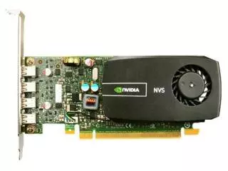
HD Graphics 630 vs NVS 510
When comparing HD Graphics 630 and NVS 510, we look primarily at benchmarks and game tests. But it is not only about the numbers. Often you can find third-party models with higher clock speeds, better cooling, or a customizable RGB lighting. Not all of them will have all the features you need. Another thing to consider is the port selection. Most graphics cards have at least one DisplayPort and HDMI interface, but some monitors require DVI. Before you buy, check the TDP of the graphics card - this characteristic will help you estimate the consumption of the graphics card. You may even have to upgrade your PSU to meet its requirements. An important factor when choosing between HD Graphics 630 and NVS 510 is the price. Does the additional cost justify the performance hit? Our comparison should help you make the right decision.
HD Graphics 630
Main Specs
HD Graphics 630
NVS 510
Power consumption (TDP)
15 Watt
35 Watt
Interface
PCIe 3.0 x1
PCIe 2.0 x16
Supplementary power connectors
None
Memory type
DDR3L/LPDDR3/LPDDR4
DDR3
Maximum RAM amount
64 GB
2 GB
Display Connectors
No outputs
4x mini-DisplayPort
Check Price
NVS 510 has 133% more power consumption, than HD Graphics 630.
HD Graphics 630 is connected by PCIe 3.0 x1, and NVS 510 uses PCIe 2.0 x16 interface.
HD Graphics 630 has 62 GB more memory, than NVS 510.
Both cards are used in Desktops.
HD Graphics 630 is build with Gen. 9.5 Kaby Lake architecture, and NVS 510 - with Kepler.
Core clock speed of NVS 510 is 497 MHz higher, than HD Graphics 630.
HD Graphics 630 is manufactured by 14 nm process technology, and NVS 510 - by 28 nm process technology.
Game benchmarks
Assassin's Creed Odyssey
Battlefield 5
Call of Duty: Warzone
Counter-Strike: Global Offensive
Cyberpunk 2077
Dota 2
Far Cry 5
Fortnite
Forza Horizon 4
Grand Theft Auto V
Metro Exodus
Minecraft
PLAYERUNKNOWN'S BATTLEGROUNDS
Red Dead Redemption 2
The Witcher 3: Wild Hunt
World of Tanks
high / 1080p
3−4
0−1
ultra / 1080p
1−2
−
QHD / 1440p
0−1
0−1
low / 720p
14−16
1−2
medium / 1080p
5−6
0−1
The average gaming FPS of HD Graphics 630 in Assassin's Creed Odyssey is 1400% more, than NVS 510.
high / 1080p
7−8
−
ultra / 1080p
5−6
−
QHD / 1440p
0−1
0−1
low / 720p
18−20
0−1
medium / 1080p
8−9
−
low / 768p
45−50
50−55
high / 1080p
40−45
45−50
QHD / 1440p
0−1
0−1
The average gaming FPS of NVS 510 in Call of Duty: Warzone is 11% more, than HD Graphics 630.
low / 768p
120−130
60−65
medium / 768p
95−100
27−30
ultra / 1080p
45−50
7−8
QHD / 1440p
24−27
−
high / 768p
70−75
16−18
The average gaming FPS of HD Graphics 630 in Counter-Strike: Global Offensive is 203% more, than NVS 510.
low / 768p
70−75
70−75
ultra / 1080p
20−22
0−1
medium / 1080p
40−45
45−50
The average gaming FPS of NVS 510 in Cyberpunk 2077 is 5% more, than HD Graphics 630.
low / 768p
75−80
45−50
medium / 768p
55−60
10−11
ultra / 1080p
27−30
0−1
The average gaming FPS of HD Graphics 630 in Dota 2 is 131% more, than NVS 510.
high / 1080p
3−4
−
ultra / 1080p
3−4
−
4K / 2160p
0−1
−
low / 720p
14−16
0−1
medium / 1080p
5−6
−
high / 1080p
12−14
−
ultra / 1080p
7−8
−
QHD / 1440p
4−5
−
low / 720p
55−60
21−24
medium / 1080p
14−16
0−1
The average gaming FPS of HD Graphics 630 in Fortnite is 159% more, than NVS 510.
high / 1080p
6−7
0−1
ultra / 1080p
6−7
−
QHD / 1440p
0−1
0−1
low / 720p
20−22
0−1
medium / 1080p
9−10
0−1
low / 768p
45−50
18−20
high / 1080p
8−9
0−1
ultra / 1080p
3−4
−
QHD / 1440p
0−1
0−1
medium / 720p
40−45
12−14
The average gaming FPS of HD Graphics 630 in Grand Theft Auto V is 181% more, than NVS 510.
high / 1080p
2−3
−
ultra / 1080p
0−1
−
4K / 2160p
0−1
−
low / 720p
7−8
0−1
medium / 1080p
3−4
−
low / 768p
85−90
75−80
high / 1080p
65−70
27−30
The average gaming FPS of HD Graphics 630 in Minecraft is 45% more, than NVS 510.
ultra / 1080p
12−14
−
low / 720p
27−30
8−9
medium / 1080p
14−16
−
The average gaming FPS of HD Graphics 630 in PLAYERUNKNOWN'S BATTLEGROUNDS is 250% more, than NVS 510.
high / 1080p
6−7
−
ultra / 1080p
4−5
−
QHD / 1440p
0−1
−
low / 720p
7−8
0−1
low / 768p
16−18
0−1
medium / 768p
12−14
−
high / 1080p
6−7
−
ultra / 1080p
4−5
−
4K / 2160p
1−2
−
low / 768p
70−75
45−50
medium / 768p
35−40
14−16
ultra / 1080p
16−18
0−1
high / 768p
30−35
12−14
The average gaming FPS of HD Graphics 630 in World of Tanks is 88% more, than NVS 510.
Full Specs
HD Graphics 630
NVS 510
Architecture
Gen. 9.5 Kaby Lake
Kepler
Code name
Kaby-Lake-H-GT2
GK107
Type
Desktop
Workstation
Release date
1 January 2017
23 October 2012
Pipelines
24
192
Core clock speed
300 MHz
797 MHz
Boost Clock
1150 MHz
Transistor count
189 million
1,270 million
Manufacturing process technology
14 nm
28 nm
Texture fill rate
26.40
12.75
Floating-point performance
441.6 gflops
306.0 gflops
Length
160 mm
Memory bus width
64/128 Bit
128 Bit
Memory clock speed
1782 MHz
Memory bandwidth
28.51 GB/s
Shared memory
+
DirectX
12 (12_1)
12 (11_0)
Shader Model
6.4
5.1
OpenGL
4.6
4.6
OpenCL
2.1
1.2
Vulkan
1.1.103
1.1.126
CUDA
3.0
Bitcoin / BTC (SHA256)
17 Mh/s
Quick Sync
+
Check Price


