Quadro FX 3800 vs Radeon Pro WX 4100
Find out if it is worth upgrading your current GPU setup by comparing Quadro FX 3800 and Radeon Pro WX 4100. Here you can take a closer look at graphics cards specs, such as core clock speed, memory type and size, display connectors, etc. The price, overall benchmark and gaming performances are usually defining factors when it comes to choosing between Quadro FX 3800 and Radeon Pro WX 4100. Make sure that the graphics card has compatible dimensions and will properly fit in your new or current computer case. Also these graphics cards may have different system power recommendations, so take that into consideration and upgrade your PSU if necessary.
Quadro FX 3800
Main Specs
Quadro FX 3800
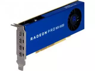
Radeon Pro WX 4100
Power consumption (TDP)
108 Watt
50 Watt
Interface
PCIe 2.0 x16
PCIe 3.0 x8
Supplementary power connectors
1x 6-pin
None
Memory type
GDDR3
GDDR5
Maximum RAM amount
1 GB
4 GB
Display Connectors
1x DVI, 2x DisplayPort
4x mini-DisplayPort
Check Price
Quadro FX 3800 has 116% more power consumption, than Radeon Pro WX 4100.
Quadro FX 3800 is connected by PCIe 2.0 x16, and Radeon Pro WX 4100 uses PCIe 3.0 x8 interface.
Radeon Pro WX 4100 has 3 GB more memory, than Quadro FX 3800.
Both cards are used in Desktops.
Quadro FX 3800 is build with Tesla 2.0 architecture, and Radeon Pro WX 4100 - with GCN 4.0.
Core clock speed of Radeon Pro WX 4100 is 525 MHz higher, than Quadro FX 3800.
Quadro FX 3800 is manufactured by 55 nm process technology, and Radeon Pro WX 4100 - by 14 nm process technology.
Memory clock speed of Radeon Pro WX 4100 is 4400 MHz higher, than Quadro FX 3800.
Game benchmarks
Assassin's Creed Odyssey
Battlefield 5
Call of Duty: Warzone
Counter-Strike: Global Offensive
Cyberpunk 2077
Dota 2
Far Cry 5
Fortnite
Forza Horizon 4
Grand Theft Auto V
Metro Exodus
Minecraft
PLAYERUNKNOWN'S BATTLEGROUNDS
Red Dead Redemption 2
The Witcher 3: Wild Hunt
World of Tanks
high / 1080p
0−1
18−20
ultra / 1080p
0−1
10−12
QHD / 1440p
0−1
5−6
4K / 2160p
−
4−5
low / 720p
10−11
35−40
medium / 1080p
1−2
21−24
The average gaming FPS of Radeon Pro WX 4100 in Assassin's Creed Odyssey is 400% more, than Quadro FX 3800.
high / 1080p
−
30−33
ultra / 1080p
2−3
24−27
QHD / 1440p
0−1
9−10
4K / 2160p
−
7−8
low / 720p
9−10
60−65
medium / 1080p
2−3
30−35
The average gaming FPS of Radeon Pro WX 4100 in Battlefield 5 is 900% more, than Quadro FX 3800.
low / 768p
50−55
50−55
high / 1080p
45−50
−
QHD / 1440p
0−1
0−1
Quadro FX 3800 and Radeon Pro WX 4100 have the same average FPS in Call of Duty: Warzone.
low / 768p
100−110
220−230
medium / 768p
75−80
190−200
ultra / 1080p
30−35
110−120
QHD / 1440p
−
75−80
4K / 2160p
9−10
40−45
high / 768p
50−55
160−170
The average gaming FPS of Radeon Pro WX 4100 in Counter-Strike: Global Offensive is 169% more, than Quadro FX 3800.
low / 768p
70−75
60−65
ultra / 1080p
12−14
45−50
medium / 1080p
45−50
55−60
The average gaming FPS of Radeon Pro WX 4100 in Cyberpunk 2077 is 25% more, than Quadro FX 3800.
low / 768p
65−70
110−120
medium / 768p
40−45
100−110
ultra / 1080p
14−16
75−80
The average gaming FPS of Radeon Pro WX 4100 in Dota 2 is 141% more, than Quadro FX 3800.
high / 1080p
1−2
21−24
ultra / 1080p
−
21−24
QHD / 1440p
−
18−20
4K / 2160p
0−1
7−8
low / 720p
7−8
45−50
medium / 1080p
2−3
24−27
The average gaming FPS of Radeon Pro WX 4100 in Far Cry 5 is 933% more, than Quadro FX 3800.
high / 1080p
−
30−33
ultra / 1080p
−
21−24
QHD / 1440p
0−1
14−16
low / 720p
40−45
110−120
medium / 1080p
4−5
65−70
The average gaming FPS of Radeon Pro WX 4100 in Fortnite is 295% more, than Quadro FX 3800.
high / 1080p
1−2
30−35
ultra / 1080p
−
24−27
QHD / 1440p
0−1
12−14
4K / 2160p
−
12−14
low / 720p
12−14
65−70
medium / 1080p
4−5
35−40
The average gaming FPS of Radeon Pro WX 4100 in Forza Horizon 4 is 650% more, than Quadro FX 3800.
low / 768p
35−40
95−100
medium / 768p
−
85−90
high / 1080p
1−2
35−40
ultra / 1080p
−
14−16
QHD / 1440p
0−1
5−6
medium / 720p
30−35
−
The average gaming FPS of Radeon Pro WX 4100 in Grand Theft Auto V is 252% more, than Quadro FX 3800.
high / 1080p
0−1
12−14
ultra / 1080p
0−1
9−10
4K / 2160p
0−1
2−3
low / 720p
1−2
35−40
medium / 1080p
−
16−18
The average gaming FPS of Radeon Pro WX 4100 in Metro Exodus is 3600% more, than Quadro FX 3800.
low / 768p
85−90
110−120
high / 1080p
50−55
−
medium / 1080p
−
110−120
The average gaming FPS of Radeon Pro WX 4100 in Minecraft is 32% more, than Quadro FX 3800.
high / 1080p
14−16
−
ultra / 1080p
12−14
14−16
low / 720p
21−24
65−70
medium / 1080p
14−16
18−20
The average gaming FPS of Radeon Pro WX 4100 in PLAYERUNKNOWN'S BATTLEGROUNDS is 106% more, than Quadro FX 3800.
high / 1080p
−
14−16
ultra / 1080p
−
9−10
QHD / 1440p
0−1
0−1
4K / 2160p
−
0−1
low / 720p
2−3
35−40
medium / 1080p
−
18−20
The average gaming FPS of Radeon Pro WX 4100 in Red Dead Redemption 2 is 1750% more, than Quadro FX 3800.
low / 768p
4−5
65−70
medium / 768p
−
40−45
high / 1080p
2−3
21−24
ultra / 1080p
−
12−14
4K / 2160p
0−1
7−8
The average gaming FPS of Radeon Pro WX 4100 in The Witcher 3: Wild Hunt is 1400% more, than Quadro FX 3800.
low / 768p
65−70
90−95
medium / 768p
30−35
60−65
ultra / 1080p
10−12
40−45
high / 768p
27−30
55−60
The average gaming FPS of Radeon Pro WX 4100 in World of Tanks is 85% more, than Quadro FX 3800.
Full Specs
Quadro FX 3800
Radeon Pro WX 4100
Architecture
Tesla 2.0
GCN 4.0
Code name
GT200B
Baffin
Type
Workstation
Workstation
Release date
30 March 2009
10 November 2016
Pipelines
192
1024
Core clock speed
600 MHz
1125 MHz
Boost Clock
1201 MHz
Transistor count
1,400 million
3,000 million
Manufacturing process technology
55 nm
14 nm
Texture fill rate
38.40
76.86
Floating-point performance
462.3 gflops
2,460 gflops
Length
198 mm
Memory bus width
256 Bit
128 Bit
Memory clock speed
1600 MHz
6000 MHz
Memory bandwidth
51.2 GB/s
96 GB/s
DirectX
11.1 (10_0)
12 (12_0)
Shader Model
4.0
6.4
OpenGL
3.3
4.6
OpenCL
1.1
2.0
Vulkan
N/A
1.2.131
CUDA
1.3
Check Price