GeForce GTX 465 vs Radeon R9 280
Find out if it is worth upgrading your current GPU setup by comparing GeForce GTX 465 and Radeon R9 280. Here you can take a closer look at graphics cards specs, such as core clock speed, memory type and size, display connectors, etc. The price, overall benchmark and gaming performances are usually defining factors when it comes to choosing between GeForce GTX 465 and Radeon R9 280. Make sure that the graphics card has compatible dimensions and will properly fit in your new or current computer case. Also these graphics cards may have different system power recommendations, so take that into consideration and upgrade your PSU if necessary.
Main Specs
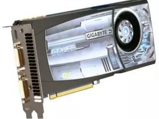
GeForce GTX 465
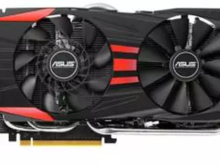
Radeon R9 280
Power consumption (TDP)
200 Watt
200 Watt
Interface
PCIe 2.0 x16
PCIe 3.0 x16
Supplementary power connectors
Two 6-pins
1 x 6-pin + 1 x 8-pin
Memory type
GDDR5
GDDR5
Maximum RAM amount
1 GB
3 GB
Display Connectors
2x DVI, 1x mini-HDMI
2x DVI, 1x HDMI, 2x mini-DisplayPort
Check Price
Check Price
Both graphics cards have the same power consumption of 200 Watt.
GeForce GTX 465 is connected by PCIe 2.0 x16, and Radeon R9 280 uses PCIe 3.0 x16 interface.
Radeon R9 280 has 2 GB more memory, than GeForce GTX 465.
Both cards are used in Desktops.
GeForce GTX 465 is build with Fermi architecture, and Radeon R9 280 - with GCN 1.0.
GeForce GTX 465 is manufactured by 40 nm process technology, and Radeon R9 280 - by 28 nm process technology.
Radeon R9 280 is 266 mm longer, than GeForce GTX 465.
Memory clock speed of GeForce GTX 465 is 353 MHz higher, than Radeon R9 280.
Game benchmarks
Assassin's Creed Odyssey
Battlefield 5
Call of Duty: Warzone
Counter-Strike: Global Offensive
Cyberpunk 2077
Dota 2
Far Cry 5
Fortnite
Forza Horizon 4
Grand Theft Auto V
Metro Exodus
Minecraft
PLAYERUNKNOWN'S BATTLEGROUNDS
Red Dead Redemption 2
The Witcher 3: Wild Hunt
World of Tanks
high / 1080p
14−16
35−40
ultra / 1080p
8−9
21−24
QHD / 1440p
3−4
16−18
4K / 2160p
−
10−11
low / 720p
30−33
60−65
medium / 1080p
18−20
40−45
The average gaming FPS of Radeon R9 280 in Assassin's Creed Odyssey is 140% more, than GeForce GTX 465.
high / 1080p
21−24
55−60
ultra / 1080p
20−22
45−50
QHD / 1440p
6−7
35−40
4K / 2160p
5−6
18−20
low / 720p
50−55
100−110
medium / 1080p
24−27
60−65
The average gaming FPS of Radeon R9 280 in Battlefield 5 is 145% more, than GeForce GTX 465.
low / 768p
45−50
50−55
QHD / 1440p
0−1
0−1
The average gaming FPS of Radeon R9 280 in Call of Duty: Warzone is 10% more, than GeForce GTX 465.
low / 768p
200−210
250−260
medium / 768p
170−180
220−230
ultra / 1080p
95−100
180−190
QHD / 1440p
50−55
110−120
4K / 2160p
30−33
70−75
high / 768p
130−140
210−220
The average gaming FPS of Radeon R9 280 in Counter-Strike: Global Offensive is 52% more, than GeForce GTX 465.
low / 768p
55−60
60−65
ultra / 1080p
35−40
−
medium / 1080p
45−50
55−60
The average gaming FPS of Radeon R9 280 in Cyberpunk 2077 is 15% more, than GeForce GTX 465.
low / 768p
100−110
120−130
medium / 768p
90−95
110−120
ultra / 1080p
60−65
100−110
The average gaming FPS of Radeon R9 280 in Dota 2 is 33% more, than GeForce GTX 465.
high / 1080p
16−18
45−50
ultra / 1080p
14−16
40−45
QHD / 1440p
−
27−30
4K / 2160p
6−7
14−16
low / 720p
35−40
80−85
medium / 1080p
18−20
45−50
The average gaming FPS of Radeon R9 280 in Far Cry 5 is 147% more, than GeForce GTX 465.
high / 1080p
24−27
60−65
ultra / 1080p
18−20
45−50
QHD / 1440p
16−18
27−30
4K / 2160p
−
27−30
low / 720p
95−100
180−190
medium / 1080p
50−55
110−120
The average gaming FPS of Radeon R9 280 in Fortnite is 107% more, than GeForce GTX 465.
high / 1080p
24−27
60−65
ultra / 1080p
18−20
45−50
QHD / 1440p
8−9
30−35
4K / 2160p
−
24−27
low / 720p
50−55
100−110
medium / 1080p
27−30
65−70
The average gaming FPS of Radeon R9 280 in Forza Horizon 4 is 142% more, than GeForce GTX 465.
low / 768p
80−85
140−150
medium / 768p
70−75
120−130
high / 1080p
27−30
70−75
ultra / 1080p
12−14
30−35
QHD / 1440p
2−3
21−24
The average gaming FPS of Radeon R9 280 in Grand Theft Auto V is 102% more, than GeForce GTX 465.
high / 1080p
9−10
24−27
ultra / 1080p
7−8
20−22
QHD / 1440p
−
16−18
4K / 2160p
2−3
8−9
low / 720p
27−30
65−70
medium / 1080p
12−14
30−35
The average gaming FPS of Radeon R9 280 in Metro Exodus is 158% more, than GeForce GTX 465.
low / 768p
110−120
130−140
ultra / 1080p
100−110
−
medium / 1080p
100−110
120−130
The average gaming FPS of Radeon R9 280 in Minecraft is 18% more, than GeForce GTX 465.
high / 1080p
21−24
−
ultra / 1080p
16−18
14−16
low / 720p
55−60
100−110
medium / 1080p
24−27
18−20
The average gaming FPS of Radeon R9 280 in PLAYERUNKNOWN'S BATTLEGROUNDS is 39% more, than GeForce GTX 465.
high / 1080p
14−16
24−27
ultra / 1080p
9−10
16−18
QHD / 1440p
0−1
10−11
4K / 2160p
−
7−8
low / 720p
27−30
65−70
medium / 1080p
16−18
35−40
The average gaming FPS of Radeon R9 280 in Red Dead Redemption 2 is 111% more, than GeForce GTX 465.
low / 768p
50−55
130−140
medium / 768p
30−35
85−90
high / 1080p
18−20
45−50
ultra / 1080p
10−11
24−27
4K / 2160p
8−9
16−18
The average gaming FPS of Radeon R9 280 in The Witcher 3: Wild Hunt is 158% more, than GeForce GTX 465.
low / 768p
100−110
90−95
medium / 768p
60−65
60−65
ultra / 1080p
30−35
50−55
high / 768p
50−55
60−65
The average gaming FPS of Radeon R9 280 in World of Tanks is 6% more, than GeForce GTX 465.
Full Specs
GeForce GTX 465
Radeon R9 280
Architecture
Fermi
GCN 1.0
Code name
GF100
Tahiti
Type
Desktop
Desktop
Release date
31 May 2010
4 March 2014
Pipelines
352
1792
Core clock speed
1215 MHz
Boost Clock
933 MHz
Transistor count
3,100 million
4,313 million
Manufacturing process technology
40 nm
28 nm
Texture fill rate
26.7 billion/sec
104.5
Floating-point performance
855.4 gflops
3,344 gflops
Length
9.5" (241 mm) (24.1 cm)
275 mm
Memory bus width
256 Bit
384 Bit
Memory clock speed
1603 MHz (3206 data rate)
1250 MHz
Memory bandwidth
102.6 GB/s
240 GB/s
DirectX
12 (11_0)
Shader Model
5.1
5.1
OpenGL
4.2
4.6
OpenCL
1.1
1.2
Vulkan
N/A
+
CUDA
+
FreeSync
+
CUDA cores
352
Bus support
PCI-E 2.0 x 16
PCIe 3.0
Height
4.376" (111 mm) (11.1 cm)
SLI options
+
Multi monitor support
+
HDMI
+
+
Maximum VGA resolution
2048x1536
Audio input for HDMI
Internal
Bitcoin / BTC (SHA256)
64 Mh/s
408 Mh/s
Eyefinity
+
HD3D
+
TrueAudio
+
Design
reference
CrossFire
+
DDMA audio
+
Ethereum / ETH (DaggerHashimoto)
21.5 Mh/s
Compute performance
30x
LiquidVR
+
TressFX
+
UVD
+
Check Price
Check Price