Quadro P400 vs Tesla C2075
When choosing between Quadro P400 and Tesla C2075, it is worth examining the specifications of the models in detail. Do they meet the recommended requirements of modern games and software? Storage capacity, form factor, TDP, available ports, warranty and manufacturer support are all important. For example, the size of a PC case can limit the maximum thickness and length of the card. Often, instead of the factory overclocked card and RGB backlight, it is better to choose a reference model with a more efficient GPU. And make sure that your current power supply unit has the correct connection pins (using adapters is not recommended). This GPUs compare tool is meant to help you to choose the best graphics card for your build. Let's find out the difference between Quadro P400 and Tesla C2075.
Main Specs
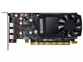
Quadro P400
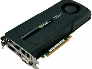
Tesla C2075
Power consumption (TDP)
30 Watt
247 Watt
Interface
PCIe 3.0 x16
PCIe 2.0 x16
Supplementary power connectors
None
1x 6-pin + 1x 8-pin
Memory type
GDDR5
GDDR5
Maximum RAM amount
2 GB
6 GB
Display Connectors
3x mini-DisplayPort
1x DVI
Check Price
Check Price
Tesla C2075 has 723% more power consumption, than Quadro P400.
Quadro P400 is connected by PCIe 3.0 x16, and Tesla C2075 uses PCIe 2.0 x16 interface.
Tesla C2075 has 4 GB more memory, than Quadro P400.
Both cards are used in Desktops.
Quadro P400 is build with Pascal architecture, and Tesla C2075 - with Fermi 2.0.
Core clock speed of Quadro P400 is 654 MHz higher, than Tesla C2075.
Quadro P400 is manufactured by 14 nm process technology, and Tesla C2075 - by 40 nm process technology.
Tesla C2075 is 103 mm longer, than Quadro P400.
Memory clock speed of Quadro P400 is 876 MHz higher, than Tesla C2075.
Game benchmarks
Assassin's Creed Odyssey
Battlefield 5
Call of Duty: Warzone
Counter-Strike: Global Offensive
Cyberpunk 2077
Dota 2
Far Cry 5
Fortnite
Forza Horizon 4
Grand Theft Auto V
Metro Exodus
Minecraft
PLAYERUNKNOWN'S BATTLEGROUNDS
Red Dead Redemption 2
The Witcher 3: Wild Hunt
World of Tanks
high / 1080p
7−8
16−18
ultra / 1080p
4−5
10−11
QHD / 1440p
0−1
4−5
low / 720p
18−20
35−40
medium / 1080p
9−10
21−24
The average gaming FPS of Tesla C2075 in Assassin's Creed Odyssey is 110% more, than Quadro P400.
high / 1080p
12−14
27−30
ultra / 1080p
10−12
21−24
QHD / 1440p
0−1
6−7
4K / 2160p
−
6−7
low / 720p
27−30
55−60
medium / 1080p
14−16
30−35
The average gaming FPS of Tesla C2075 in Battlefield 5 is 118% more, than Quadro P400.
low / 768p
45−50
50−55
high / 1080p
45−50
50−55
QHD / 1440p
0−1
0−1
The average gaming FPS of Tesla C2075 in Call of Duty: Warzone is 10% more, than Quadro P400.
low / 768p
140−150
210−220
medium / 768p
110−120
190−200
ultra / 1080p
55−60
100−110
QHD / 1440p
30−35
65−70
4K / 2160p
27−30
30−35
high / 768p
85−90
150−160
The average gaming FPS of Tesla C2075 in Counter-Strike: Global Offensive is 66% more, than Quadro P400.
low / 768p
55−60
60−65
ultra / 1080p
21−24
45−50
medium / 1080p
45−50
55−60
The average gaming FPS of Tesla C2075 in Cyberpunk 2077 is 30% more, than Quadro P400.
low / 768p
85−90
110−120
medium / 768p
60−65
100−110
ultra / 1080p
35−40
70−75
The average gaming FPS of Tesla C2075 in Dota 2 is 56% more, than Quadro P400.
high / 1080p
9−10
21−24
ultra / 1080p
8−9
18−20
QHD / 1440p
−
18−20
4K / 2160p
4−5
6−7
low / 720p
21−24
45−50
medium / 1080p
10−11
21−24
The average gaming FPS of Tesla C2075 in Far Cry 5 is 109% more, than Quadro P400.
high / 1080p
16−18
27−30
ultra / 1080p
10−12
21−24
QHD / 1440p
−
14−16
low / 720p
65−70
110−120
medium / 1080p
24−27
60−65
The average gaming FPS of Tesla C2075 in Fortnite is 90% more, than Quadro P400.
high / 1080p
12−14
27−30
ultra / 1080p
12−14
21−24
QHD / 1440p
2−3
10−11
low / 720p
27−30
60−65
medium / 1080p
14−16
30−35
The average gaming FPS of Tesla C2075 in Forza Horizon 4 is 121% more, than Quadro P400.
low / 768p
55−60
90−95
medium / 768p
45−50
80−85
high / 1080p
14−16
30−35
ultra / 1080p
7−8
14−16
QHD / 1440p
0−1
4−5
The average gaming FPS of Tesla C2075 in Grand Theft Auto V is 77% more, than Quadro P400.
high / 1080p
5−6
10−12
ultra / 1080p
3−4
8−9
4K / 2160p
0−1
1−2
low / 720p
14−16
30−35
medium / 1080p
7−8
14−16
The average gaming FPS of Tesla C2075 in Metro Exodus is 128% more, than Quadro P400.
low / 768p
95−100
110−120
high / 1080p
90−95
−
ultra / 1080p
80−85
−
medium / 1080p
95−100
110−120
The average gaming FPS of Tesla C2075 in Minecraft is 18% more, than Quadro P400.
high / 1080p
16−18
−
ultra / 1080p
14−16
14−16
low / 720p
35−40
60−65
medium / 1080p
18−20
18−20
The average gaming FPS of Tesla C2075 in PLAYERUNKNOWN'S BATTLEGROUNDS is 39% more, than Quadro P400.
high / 1080p
−
14−16
ultra / 1080p
8−9
9−10
QHD / 1440p
0−1
0−1
low / 720p
14−16
30−35
medium / 1080p
10−12
18−20
The average gaming FPS of Tesla C2075 in Red Dead Redemption 2 is 81% more, than Quadro P400.
low / 768p
27−30
60−65
medium / 768p
18−20
35−40
high / 1080p
10−11
21−24
ultra / 1080p
7−8
12−14
4K / 2160p
6−7
7−8
The average gaming FPS of Tesla C2075 in The Witcher 3: Wild Hunt is 100% more, than Quadro P400.
low / 768p
85−90
90−95
medium / 768p
45−50
60−65
ultra / 1080p
21−24
35−40
high / 768p
35−40
55−60
The average gaming FPS of Tesla C2075 in World of Tanks is 29% more, than Quadro P400.
Full Specs
Quadro P400
Tesla C2075
Architecture
Pascal
Fermi 2.0
Code name
GP107
GF110
Type
Workstation
Workstation
Release date
7 February 2017
25 July 2011
Pipelines
256
448
Core clock speed
1228 MHz
574 MHz
Boost Clock
1252 MHz
Transistor count
3,300 million
3,000 million
Manufacturing process technology
14 nm
40 nm
Texture fill rate
20.03
32.14
Floating-point performance
679.9 gflops
1,030.4 gflops
Length
145 mm
248 mm
Memory bus width
64 Bit
384 Bit
Memory clock speed
4008 MHz
3132 MHz
Memory bandwidth
32.06 GB/s
150.3 GB/s
DirectX
12 (12_1)
12 (11_0)
Shader Model
6.4
5.1
OpenGL
4.6
4.6
OpenCL
1.2
1.1
Vulkan
1.2.131
N/A
CUDA
6.1
2.0
Bitcoin / BTC (SHA256)
94 Mh/s
Check Price
Check Price