Samsung's zHBM stacks memory on top of AI chips to promise 8x the speed of HBM5

Samsung showed up to the Future of Memory and Storage (FMS) 2026 conference with its most ambitious memory roadmap in years. The centerpiece is zHBM—a vertical stacking architecture that places memory directly on top of an AI accelerator chip rather than beside it—claiming 8x the performance of HBM5, 10x the density, and 50% lower thermal resistance. None of it is in production yet, but the direction is clear: Samsung wants to reclaim the AI memory lead it lost to SK Hynix.
The vertical bet
Today's HBM (High Bandwidth Memory) sits next to a GPU or AI accelerator on a shared substrate. Samsung's zHBM concept cuts the signal path dramatically by stacking memory wafers directly above the compute die using wafer-bonding techniques. According to Samsung Newsroom, the theoretical gains are striking: 8x HBM5 performance, 10x density improvement, and 3x better power efficiency. Samsung itself flags these as engineering projections, not measured results from physical silicon.
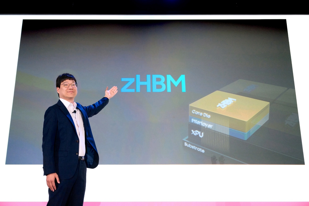
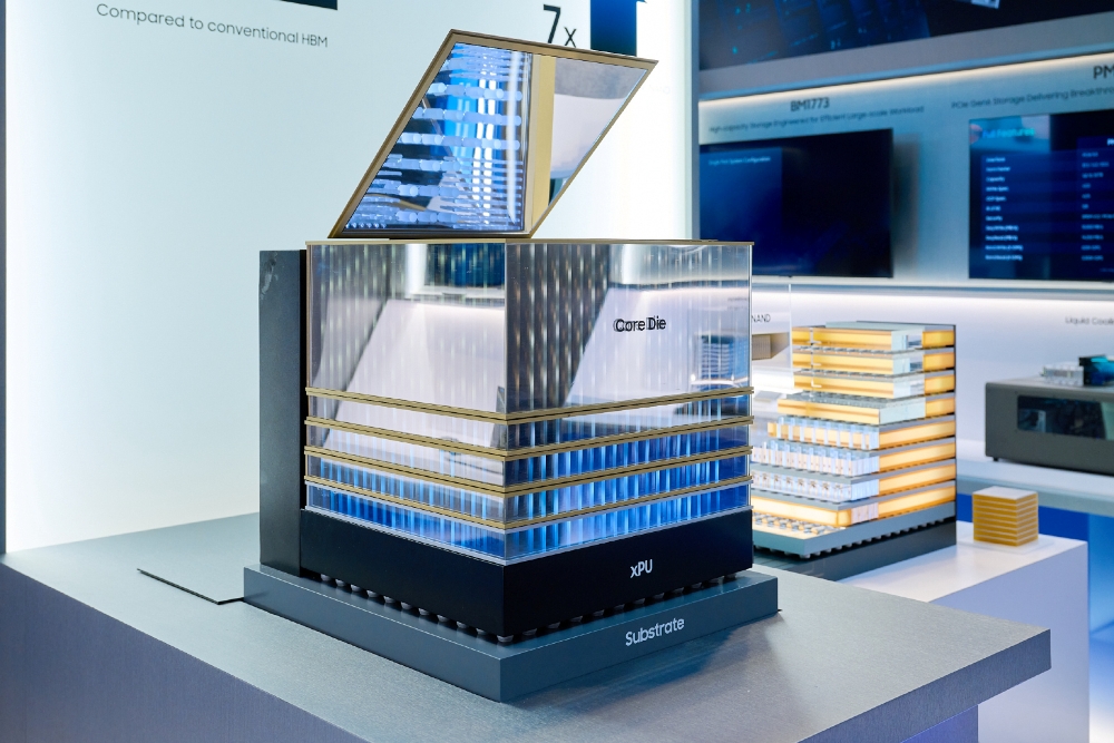
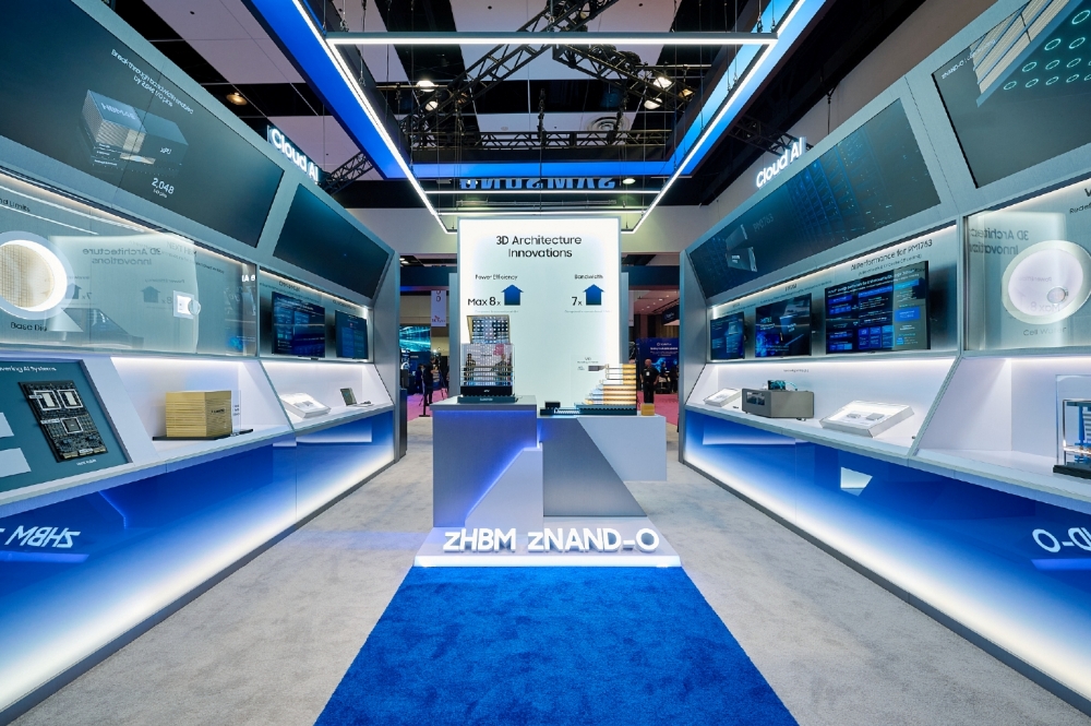





The thermal reduction figure—50% less resistance—matters most for real-world data center operators. AI servers already burn through hundreds of watts per accelerator; anything that keeps chips cooler at scale is worth watching.
The NAND race and what's shipping now
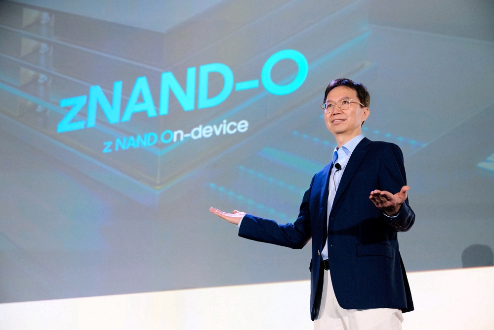
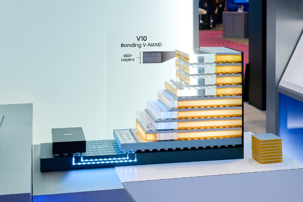
Alongside zHBM, Samsung revealed the V10 Bonding V-NAND prototype, which exceeds 400 layers. The trick is a wafer-bonding process (BV-NAND) that manufactures the memory cell array and control logic on separate wafers, then bonds them together. The result is a 58% density jump over the current V9 generation, per StorageReview. Samsung also floated zNAND-O, a low-latency NAND concept aimed at AI edge systems that need to process data locally.
On the products-you-can-actually-buy side, Samsung confirmed mass production of the PM1763 and BM1773 enterprise SSDs, and began shipping samples of its LPDDR5X-PIM—an industry-first LPDDR memory module with processing-in-memory capability that offloads compute tasks from the main processor. HBM4 has been in mass production since February 2026, with HBM4E samples shipping from May 2026.
Caveats worth noting
The bigger concepts—zHBM and zNAND-O—have no announced production timeline and no confirmed compatibility with NVIDIA or AMD accelerators. No third-party validation has been announced. SK Hynix is developing a competing 375-layer V10 4D NAND with earlier production targets, and Intel holds patents in adjacent vertical memory territory. Samsung is rebuilding its position in the AI memory market, but the gap between concept and chip fab is wide. Data center operators should treat today's announcements as a directional signal, not a procurement decision.


